Revolutionary DTU Nanolaser Breakthrough Paves the Way for Light-Based Microchips and Ultra-Efficient Computing

Researchers at the Technical University of Denmark (DTU) have unveiled a groundbreaking nanolaser that could fundamentally alter the landscape of modern computing, telecommunications, and healthcare diagnostics. Published in the peer-reviewed scientific journal Science Advances, this technological leap marks a pivotal milestone toward an era where microchips communicate entirely through particles of light rather than traditional electrical currents. Led by a team of visionary scientists from DTU Electro—including Professor Jesper Mørk alongside Drs. Meng Xiong and Yi Yu—the innovation successfully pushes the boundaries of miniaturization, tackling fundamental physical constraints that have stymied semiconductor research for decades.
As global demand for computational power skyrockets, driven by artificial intelligence, cloud computing, and massive data centers, traditional electronics face a compounding crisis. The physical limitations of copper wires and electrical resistance generate significant heat and energy loss, bottlenecking data transmission speeds. By shifting the paradigm from electrons to photons, this newly developed DTU nanolaser offers a credible, scalable pathway to faster, cooler, and substantially more energy-efficient digital infrastructure.
The Main Facts of the Breakthrough
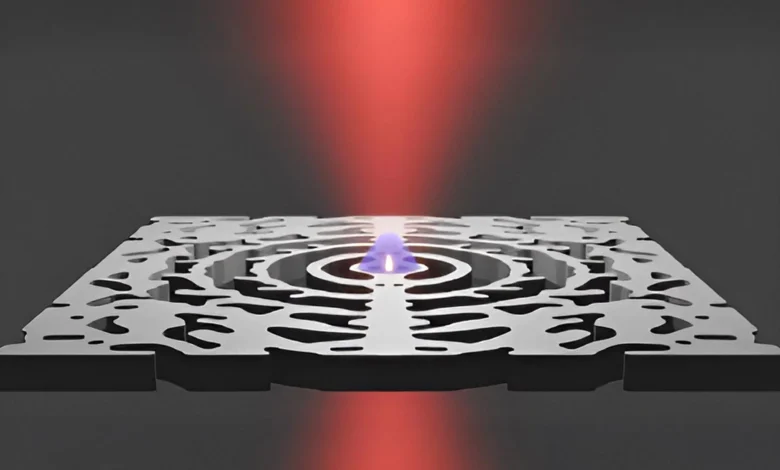
At the core of the DTU discovery is an exceptionally compact nanolaser engineered within the advanced cleanroom facilities of DTU Nanolab. Unlike conventional lasers that require bulky resonant cavities, this device relies on an advanced nanocavity structure designed to trap and concentrate light within an infinitesimally small footprint. The foundational design of this light-trapping architecture originated from pioneering work by Professor Ole Sigmund’s research group at DTU Construct, showcasing a successful multidisciplinary collaboration across university departments.
When a targeted beam of light is shone onto the device, both photons and electrons are tightly confined within the same microscopic region. This intense spatial concentration enables the nanolaser to operate efficiently at room temperature while consuming remarkably low levels of energy. By shrinking the laser cavity close to the fundamental diffraction limit, the researchers have achieved a breakthrough that bridges the gap between macroscopic optical systems and nanoscale electronic components.
The primary innovation lies in the device’s ability to seamlessly integrate high optical confinement with low operational thresholds. In practical terms, this means thousands of these microscopic lasers could theoretically be etched onto a single silicon microchip. Instead of relying on copper interconnects to shuttle data via electrical pulses across a processor—a process plagued by RC delay and thermal dissipation—future computing architectures could utilize microscopic optical pathways. Photons can travel at unprecedented speeds with virtually zero resistance-based energy loss, radically transforming how microprocessors process information.
A Chronological Timeline of Optical Computing Research
To fully appreciate the significance of the DTU nanolaser, it is essential to examine the historical trajectory of silicon photonics and optical interconnects. The quest to replace electrons with photons inside computers is not new; it is a multi-decade endeavor pursued by academia and industrial giants alike.
During the late 20th century, telecommunications underwent a massive revolution as fiber-optic networks replaced copper cables globally. Light became the undisputed champion of long-distance data transmission due to its immense bandwidth and negligible attenuation. However, scaling this technology down to the microchip level remained an elusive dream. While optical fibers could span continents, routing light around a piece of silicon measuring just a few square centimeters presented formidable manufacturing and physical hurdles.
In the 2000s, researchers began developing silicon photonics, attempting to etch optical components directly onto standard semiconductor wafers. Major technology corporations and academic labs achieved milestones in creating optical modulators and germanium-on-silicon photodetectors. Yet, a major bottleneck persisted: the lack of an efficient, nanoscale laser source that could be directly integrated onto silicon chips without requiring cryogenic cooling or excessive power consumption. Most lasers were simply too large to be packed densely onto microprocessors, and those that were miniaturized suffered from high optical losses and poor energy efficiency.
Throughout the 2010s, advancements in nanofabrication and inverse design algorithms—such as those pioneered by DTU Construct—began to change the equation. Scientists started utilizing complex mathematical optimization to design non-intuitive, highly efficient light-trapping nanocavities.
By the early 2020s, the convergence of advanced cleanroom capabilities and multidisciplinary collaboration at institutions like DTU set the stage for the current breakthrough. The publication in Science Advances represents the culmination of years of iterative design, simulation, and physical fabrication, moving nanolasers out of theoretical physics journals and into tangible, functional prototypes.
Supporting Data and Technical Specifications
The implications of the DTU nanolaser are best understood through the lens of thermodynamic efficiency and data scaling. Modern microprocessors contain billions of transistors operating at gigahertz frequencies. As Moore’s Law encounters physical and economic roadblocks, energy dissipation has become the primary constraint on computing performance. Data centers worldwide now consume staggering amounts of electricity—rivaling the power consumption of entire nations—largely dedicated to powering servers and keeping them cool.
According to preliminary estimates by Professor Jesper Mørk and his research colleagues, the widespread adoption of nanolaser-based optical interconnects within consumer computers and enterprise servers could slash overall device energy consumption by up to 50 percent. This dramatic reduction stems from two distinct factors: the elimination of resistive heating in microchip wiring and the inherently lower energy per bit required to transmit optical signals versus electrical ones.
Furthermore, the physical dimensions of the DTU nanolaser operate on a scale measured in fractions of a micrometer. This ultra-compact footprint allows for an unprecedented integration density. While traditional off-chip laser diodes occupy square millimeters of space, the DTU device reduces this footprint by orders of magnitude, making on-chip dense wavelength-division multiplexing (DWDM) a viable engineering target. By multiplexing multiple wavelengths of light through a single microscopic channel on a chip, data bandwidth could be scaled exponentially without increasing physical wiring complexity.
Official Responses and Scientific Reactions
The unveiling of the DTU nanolaser has generated considerable enthusiasm within the international photonics and semiconductor research communities. Independent experts note that while many nanolasers have been demonstrated in laboratory settings in the past, few have managed to combine room-temperature operation with the ultra-low thresholds and scalable fabrication potential exhibited by the Danish team.
"The nanolaser opens up the possibility of creating a new generation of components that combine high performance with minimal size," states Professor Jesper Mørk, underscoring the versatility of the technology. Mørk and his co-authors, Drs. Meng Xiong and Yi Yu, emphasize that the design’s compatibility with standard semiconductor fabrication processes is a critical factor for eventual commercialization.
Colleagues in materials science and electrical engineering have similarly lauded the cross-disciplinary approach that married advanced mathematical optimization—courtesy of Professor Ole Sigmund’s group—with state-of-the-art cleanroom nanofabrication. By utilizing advanced topology optimization techniques, the DTU team was able to engineer a nanocavity geometry that maximizes light-matter interaction far beyond what manual design iterations could achieve.
Broader Impact and Industrial Implications
The ramifications of integrating lasers directly onto microchips extend far beyond consumer electronics, touching upon diverse sectors including enterprise computing, telecommunications, and advanced healthcare technology.
In the realm of personal computing and mobile devices, the integration of nanolasers could herald a new golden era of battery efficiency and processing power. Smartphones could execute complex artificial intelligence models locally without generating excessive thermal throttling or draining batteries within hours. Laptops and tablets could achieve workstation-level performance while maintaining fanless, silent designs.
At the enterprise level, hyperscale data centers operated by technology giants could experience transformative cost and energy savings. Cooling infrastructure—currently a massive capital and operational expense—could be significantly downsized as the internal heat generation of processors plummets. This reduction in energy demand aligns closely with global corporate sustainability goals and international carbon-reduction mandates.
Meanwhile, the healthcare sector stands to gain immensely from the extreme light concentration capabilities of the DTU nanolaser. Medical diagnostic equipment relies increasingly on optical biosensors and high-resolution imaging systems. By leveraging the ultra-small footprint and high-intensity output of nanolasers, biomedical engineers can develop portable, highly sensitive lab-on-a-chip devices capable of detecting disease biomarkers at unprecedented concentrations. These ultrasensitive biosensors could facilitate early diagnostics for oncological and infectious diseases, transforming point-of-care medical testing.
Roadmap to Commercialization: Challenges and Future Outlook
Despite the profound promise of the DTU breakthrough, researchers emphasize that significant technical milestones remain before nanolaser-powered microchips become a commercial reality.
The immediate next frontier for Professor Mørk’s team is transitioning the nanolaser from optical pumping—where an external laser beam triggers the device—to electrical pumping. For the technology to be viable inside a commercial microprocessor or smartphone, the nanolaser must be driven directly by electrical currents applied via standard semiconductor contacts. Achieving efficient electrical injection without introducing excessive heat or optical absorption losses is a notoriously difficult engineering challenge that has occupied the photonics community for years.
In addition to electrical integration, researchers must ensure long-term operational reliability and scalable manufacturing yields. Fabricating billions of error-free nanolasers across large 300-millimeter silicon wafers will require close cooperation with commercial semiconductor foundries and equipment manufacturers.
Industry analysts and academic researchers project a realistic development timeline of 5 to 10 years before the first commercial iterations of optical-interconnect microchips enter mass production. During this window, foundational research will gradually shift toward applied engineering, reliability testing, and design-software integration.
Conclusion
The development of the DTU nanolaser represents a masterclass in multidisciplinary scientific innovation, bridging theoretical physics, advanced mathematics, and cutting-edge nanofabrication. By successfully breaking conventional size limits and achieving efficient room-temperature light confinement, the team at the Technical University of Denmark has brought the long-sought dream of optical microchips closer to reality.
As the digital world confronts mounting energy crises and physical performance bottlenecks, technologies that harness the speed and efficiency of light will ultimately define the next century of computing. While hurdles such as electrical integration remain, the DTU breakthrough provides a shining beacon—quite literally—of how future generations will process information, power our global infrastructure, and advance human health.